
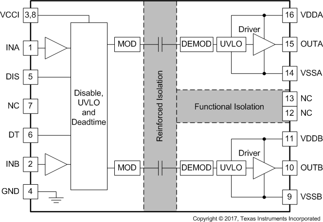
Number of channels: 2
Isolation rating: Reinforced
Withstand isolation voltage (VISO) (Vrms): 5700
Working isolation voltage (VIOWM) (Vrms): 2121
Transient isolation voltage (VIOTM) (VPK): 8000
TI functional safety category: Functional Safety Quality-Managed
Power switch: IGBT, MOSFET, SiCFET
Peak output current (A): 6
Features: Disable, Programmable dead time
Output VCC/VDD (max) (V): 25
Output VCC/VDD (min) (V): 6.5, 9.2
Input supply voltage (min) (V): 3
Input supply voltage (max) (V): 18
Propagation delay time (µs): 0.019
Input threshold: CMOS, TTL
Operating temperature range (°C): -40 to 125
Rating: Automotive
Bootstrap supply voltage (max) (V): 2121
Rise time (ns): 6
Fall time (ns): 8
更多
Undervoltage lockout (typ) (V): 5, 8
Number of channels: 2
Isolation rating: Reinforced
Withstand isolation voltage (VISO) (Vrms): 5700
Working isolation voltage (VIOWM) (Vrms): 2121
Transient isolation voltage (VIOTM) (VPK): 8000
TI functional safety category: Functional Safety Quality-Managed
Power switch: IGBT, MOSFET, SiCFET
Peak output current (A): 6
Features: Disable, Programmable dead time
Output VCC/VDD (max) (V): 25
Output VCC/VDD (min) (V): 6.5, 9.2
Input supply voltage (min) (V): 3
Input supply voltage (max) (V): 18
Propagation delay time (µs): 0.019
Input threshold: CMOS, TTL
Operating temperature range (°C): -40 to 125
Rating: Automotive
Bootstrap supply voltage (max) (V): 2121
Rise time (ns): 6
Fall time (ns): 8
Undervoltage lockout (typ) (V): 5, 8
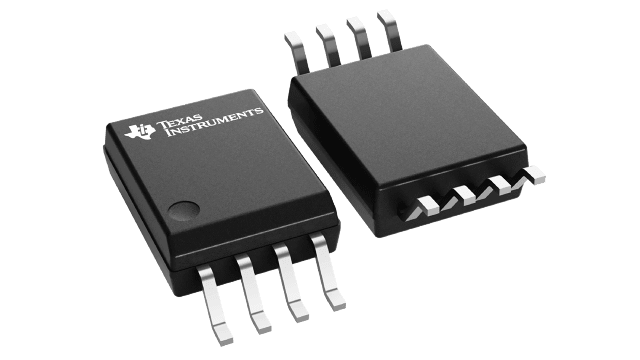
UCC5350

数据:
分类: 微电路 / 半导体集成电路 / 接口电路 / 驱动器
描述: 具有米勒钳位或分离输出以及 8V 或 12V UVLO 的 3kVrms、5A/5A 单通道隔离式栅极驱动器
Number of channels: 1
Isolation rating: Basic, Reinforced
Withstand isolation voltage (VISO) (Vrms): 3000, 5000
Working isolation voltage (VIOWM) (Vrms): 990, 2121
Transient isolation voltage (VIOTM) (VPK): 4242, 7000
Power switch: GaNFET, IGBT, MOSFET, SiCFET
Peak output current (A): 10
Features: Active miller clamp, Split output
Output VCC/VDD (max) (V): 33
Output VCC/VDD (min) (V): 9.5
Input supply voltage (min) (V): 3
Input supply voltage (max) (V): 15
Propagation delay time (µs): 0.065
Input threshold: CMOS
Operating temperature range (°C): -40 to 125
Rating: Catalog
Bootstrap supply voltage (max) (V): 2121
Rise time (ns): 10
Fall time (ns): 10
Undervoltage lockout (typ) (V): 8, 12
更多
Number of channels: 1
Isolation rating: Basic, Reinforced
Withstand isolation voltage (VISO) (Vrms): 3000, 5000
Working isolation voltage (VIOWM) (Vrms): 990, 2121
Transient isolation voltage (VIOTM) (VPK): 4242, 7000
Power switch: GaNFET, IGBT, MOSFET, SiCFET
Peak output current (A): 10
Features: Active miller clamp, Split output
Output VCC/VDD (max) (V): 33
Output VCC/VDD (min) (V): 9.5
Input supply voltage (min) (V): 3
Input supply voltage (max) (V): 15
Propagation delay time (µs): 0.065
Input threshold: CMOS
Operating temperature range (°C): -40 to 125
Rating: Catalog
Bootstrap supply voltage (max) (V): 2121
Rise time (ns): 10
Fall time (ns): 10
Undervoltage lockout (typ) (V): 8, 12
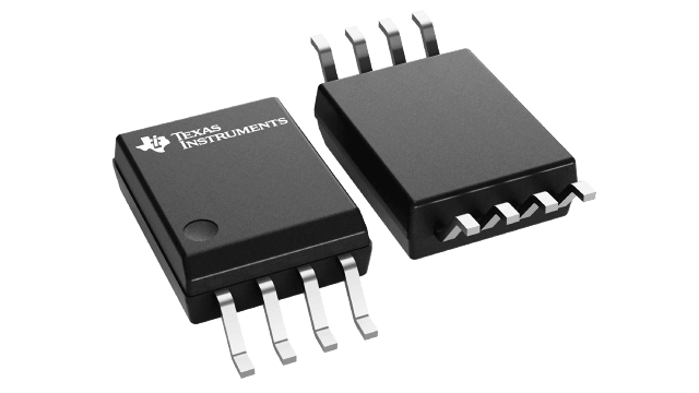
UCC5390
数据:
分类: 微电路 / 半导体集成电路 / 接口电路 / 驱动器
描述: 具有 UVLO(以 GND 为基准)或分离输出的 3kVrms/5kVrms、±10A 单通道隔离式栅极驱动器
Number of channels: 1
Isolation rating: Basic, Reinforced
Withstand isolation voltage (VISO) (Vrms): 3000, 5000
Working isolation voltage (VIOWM) (Vrms): 990, 2121
Transient isolation voltage (VIOTM) (VPK): 4242, 7000
Power switch: IGBT, MOSFET, SiCFET
Peak output current (A): 17
Features: Active miller clamp, Emitter-referenced UVLO, Split output
Output VCC/VDD (max) (V): 33
Output VCC/VDD (min) (V): 13.2
Input supply voltage (min) (V): 3
Input supply voltage (max) (V): 15
Propagation delay time (µs): 0.065
Input threshold: CMOS
Operating temperature range (°C): -40 to 125
Rating: Catalog
Bootstrap supply voltage (max) (V): 2121
Rise time (ns): 10
Fall time (ns): 10
Undervoltage lockout (typ) (V): 12
更多
Number of channels: 1
Isolation rating: Basic, Reinforced
Withstand isolation voltage (VISO) (Vrms): 3000, 5000
Working isolation voltage (VIOWM) (Vrms): 990, 2121
Transient isolation voltage (VIOTM) (VPK): 4242, 7000
Power switch: IGBT, MOSFET, SiCFET
Peak output current (A): 17
Features: Active miller clamp, Emitter-referenced UVLO, Split output
Output VCC/VDD (max) (V): 33
Output VCC/VDD (min) (V): 13.2
Input supply voltage (min) (V): 3
Input supply voltage (max) (V): 15
Propagation delay time (µs): 0.065
Input threshold: CMOS
Operating temperature range (°C): -40 to 125
Rating: Catalog
Bootstrap supply voltage (max) (V): 2121
Rise time (ns): 10
Fall time (ns): 10
Undervoltage lockout (typ) (V): 12
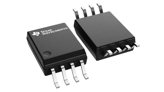
UCC5310
数据:
分类: 微电路 / 半导体集成电路 / 接口电路 / 驱动器
描述: 具有米勒钳位、12V UVLO 且采用 D 或 DWV 封装的 3kVrms/5kVrms、2A/1A 单通道隔离式栅极驱动器
Number of channels: 1
Isolation rating: Basic, Reinforced
Withstand isolation voltage (VISO) (Vrms): 3000, 5000
Working isolation voltage (VIOWM) (Vrms): 990, 2121
Transient isolation voltage (VIOTM) (VPK): 4242, 7000
Power switch: IGBT, MOSFET, SiCFET
Peak output current (A): 2.2
Features: Active miller clamp
Output VCC/VDD (max) (V): 33
Output VCC/VDD (min) (V): 13.2
Input supply voltage (min) (V): 3
Input supply voltage (max) (V): 15
Propagation delay time (µs): 0.06
Input threshold: CMOS
Operating temperature range (°C): -40 to 125
Rating: Catalog
Bootstrap supply voltage (max) (V): 2121
Rise time (ns): 12
Fall time (ns): 10
Undervoltage lockout (typ) (V): 12
更多
Number of channels: 1
Isolation rating: Basic, Reinforced
Withstand isolation voltage (VISO) (Vrms): 3000, 5000
Working isolation voltage (VIOWM) (Vrms): 990, 2121
Transient isolation voltage (VIOTM) (VPK): 4242, 7000
Power switch: IGBT, MOSFET, SiCFET
Peak output current (A): 2.2
Features: Active miller clamp
Output VCC/VDD (max) (V): 33
Output VCC/VDD (min) (V): 13.2
Input supply voltage (min) (V): 3
Input supply voltage (max) (V): 15
Propagation delay time (µs): 0.06
Input threshold: CMOS
Operating temperature range (°C): -40 to 125
Rating: Catalog
Bootstrap supply voltage (max) (V): 2121
Rise time (ns): 12
Fall time (ns): 10
Undervoltage lockout (typ) (V): 12
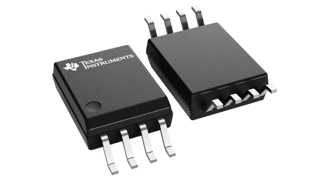
Number of channels: 1
Isolation rating: Basic, Reinforced
Withstand isolation voltage (VISO) (Vrms): 3000, 5000
Working isolation voltage (VIOWM) (Vrms): 990, 2121
Transient isolation voltage (VIOTM) (VPK): 4242, 7000
Power switch: IGBT, MOSFET, SiCFET
Peak output current (A): 4.4
Features: Emitter-referenced UVLO, Split output
Output VCC/VDD (max) (V): 33
Output VCC/VDD (min) (V): 13.2
Input supply voltage (min) (V): 3
Input supply voltage (max) (V): 15
Propagation delay time (µs): 0.06
Input threshold: CMOS
Operating temperature range (°C): -40 to 125
Rating: Automotive, Catalog
Bootstrap supply voltage (max) (V): 2121
Rise time (ns): 12
Fall time (ns): 10
Undervoltage lockout (typ) (V): 12
更多
Number of channels: 1
Isolation rating: Basic, Reinforced
Withstand isolation voltage (VISO) (Vrms): 3000, 5000
Working isolation voltage (VIOWM) (Vrms): 990, 2121
Transient isolation voltage (VIOTM) (VPK): 4242, 7000
Power switch: IGBT, MOSFET, SiCFET
Peak output current (A): 4.4
Features: Emitter-referenced UVLO, Split output
Output VCC/VDD (max) (V): 33
Output VCC/VDD (min) (V): 13.2
Input supply voltage (min) (V): 3
Input supply voltage (max) (V): 15
Propagation delay time (µs): 0.06
Input threshold: CMOS
Operating temperature range (°C): -40 to 125
Rating: Automotive, Catalog
Bootstrap supply voltage (max) (V): 2121
Rise time (ns): 12
Fall time (ns): 10
Undervoltage lockout (typ) (V): 12
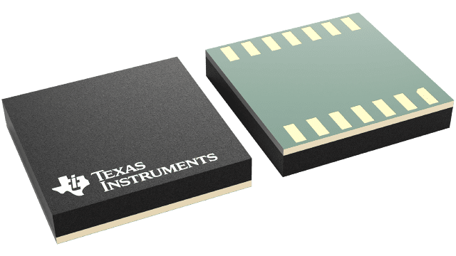
UCC20225
数据:
分类: 微电路 / 半导体集成电路 / 接口电路 / 驱动器
描述: 具有单 PWM 输入、8V UVLO 且采用 LGA 封装的 2.5kVrms、4A/6A 双通道隔离式栅极驱动器
Number of channels: 2
Isolation rating: Functional
Withstand isolation voltage (VISO) (Vrms): 2500
Working isolation voltage (VIOWM) (Vrms): 792
Transient isolation voltage (VIOTM) (VPK): 3535
Power switch: IGBT, MOSFET, SiCFET
Peak output current (A): 6
Features: Disable, Programmable dead time
Output VCC/VDD (max) (V): 25
Output VCC/VDD (min) (V): 9.2
Input supply voltage (min) (V): 3
Input supply voltage (max) (V): 18
Propagation delay time (µs): 0.019
Input threshold: CMOS, TTL
Operating temperature range (°C): -40 to 125
Rating: Catalog
Bootstrap supply voltage (max) (V): 792
Rise time (ns): 6
Fall time (ns): 7
Undervoltage lockout (typ) (V): 8
更多
Number of channels: 2
Isolation rating: Functional
Withstand isolation voltage (VISO) (Vrms): 2500
Working isolation voltage (VIOWM) (Vrms): 792
Transient isolation voltage (VIOTM) (VPK): 3535
Power switch: IGBT, MOSFET, SiCFET
Peak output current (A): 6
Features: Disable, Programmable dead time
Output VCC/VDD (max) (V): 25
Output VCC/VDD (min) (V): 9.2
Input supply voltage (min) (V): 3
Input supply voltage (max) (V): 18
Propagation delay time (µs): 0.019
Input threshold: CMOS, TTL
Operating temperature range (°C): -40 to 125
Rating: Catalog
Bootstrap supply voltage (max) (V): 792
Rise time (ns): 6
Fall time (ns): 7
Undervoltage lockout (typ) (V): 8
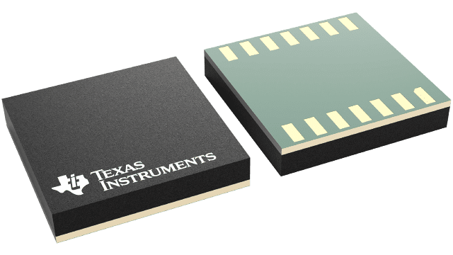
UCC21225A
数据:
分类: 微电路 / 半导体集成电路 / 接口电路 / 驱动器
描述: 具有双输入、5V UVLO 且采用 LGA 封装的 2.5kVrms、4A/6A 双通道隔离式栅极驱动器
Number of channels: 2
Isolation rating: Functional
Withstand isolation voltage (VISO) (Vrms): 2500
Working isolation voltage (VIOWM) (Vrms): 792
Transient isolation voltage (VIOTM) (VPK): 3535
Power switch: GaNFET, IGBT, MOSFET, SiCFET
Peak output current (A): 6
Features: Disable, Programmable dead time
Output VCC/VDD (max) (V): 25
Output VCC/VDD (min) (V): 6.5
Input supply voltage (min) (V): 3
Input supply voltage (max) (V): 18
Propagation delay time (µs): 0.019
Input threshold: CMOS, TTL
Operating temperature range (°C): -40 to 125
Rating: Catalog
Bootstrap supply voltage (max) (V): 792
Rise time (ns): 6
Fall time (ns): 7
Undervoltage lockout (typ) (V): 5
更多
Number of channels: 2
Isolation rating: Functional
Withstand isolation voltage (VISO) (Vrms): 2500
Working isolation voltage (VIOWM) (Vrms): 792
Transient isolation voltage (VIOTM) (VPK): 3535
Power switch: GaNFET, IGBT, MOSFET, SiCFET
Peak output current (A): 6
Features: Disable, Programmable dead time
Output VCC/VDD (max) (V): 25
Output VCC/VDD (min) (V): 6.5
Input supply voltage (min) (V): 3
Input supply voltage (max) (V): 18
Propagation delay time (µs): 0.019
Input threshold: CMOS, TTL
Operating temperature range (°C): -40 to 125
Rating: Catalog
Bootstrap supply voltage (max) (V): 792
Rise time (ns): 6
Fall time (ns): 7
Undervoltage lockout (typ) (V): 5
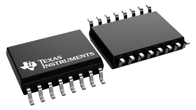
Number of channels: 1
Isolation rating: Reinforced
Withstand isolation voltage (VISO) (Vrms): 5700
Working isolation voltage (VIOWM) (Vrms): 2121
Transient isolation voltage (VIOTM) (VPK): 8000
Power switch: IGBT, MOSFET, SiCFET
Peak output current (A): 5
Output VCC/VDD (max) (V): 30
Output VCC/VDD (min) (V): 15
Input supply voltage (min) (V): 2.25
Input supply voltage (max) (V): 5.5
Propagation delay time (µs): 0.076
Input threshold: CMOS
Operating temperature range (°C): -55 to 125
Rating: HiRel Enhanced Product
Bootstrap supply voltage (max) (V): 2121
Rise time (ns): 18
Fall time (ns): 20
Undervoltage lockout (typ) (V): 12
Number of channels: 1
更多
Isolation rating: Reinforced
Withstand isolation voltage (VISO) (Vrms): 5700
Working isolation voltage (VIOWM) (Vrms): 2121
Transient isolation voltage (VIOTM) (VPK): 8000
Power switch: IGBT, MOSFET, SiCFET
Peak output current (A): 5
Output VCC/VDD (max) (V): 30
Output VCC/VDD (min) (V): 15
Input supply voltage (min) (V): 2.25
Input supply voltage (max) (V): 5.5
Propagation delay time (µs): 0.076
Input threshold: CMOS
Operating temperature range (°C): -55 to 125
Rating: HiRel Enhanced Product
Bootstrap supply voltage (max) (V): 2121
Rise time (ns): 18
Fall time (ns): 20
Undervoltage lockout (typ) (V): 12
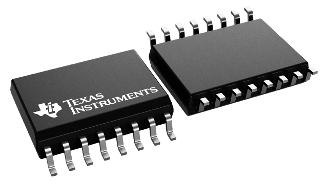
UCC20520
数据:
分类: 微电路 / 半导体集成电路 / 接口电路 / 驱动器
描述: 具有单输入、8V UVLO 且采用 LGA 封装的 5.7kVrms、4A/6A 双通道隔离式栅极驱动器
Number of channels: 2
Isolation rating: Reinforced
Withstand isolation voltage (VISO) (Vrms): 5700
Working isolation voltage (VIOWM) (Vrms): 2121
Transient isolation voltage (VIOTM) (VPK): 8000
Power switch: IGBT, MOSFET, SiCFET
Peak output current (A): 6
Features: Disable, Programmable dead time
Output VCC/VDD (max) (V): 25
Output VCC/VDD (min) (V): 9.2
Input supply voltage (min) (V): 3
Input supply voltage (max) (V): 18
Propagation delay time (µs): 0.019
Input threshold: CMOS, TTL
Operating temperature range (°C): -40 to 125
Rating: Catalog
Bootstrap supply voltage (max) (V): 2121
Rise time (ns): 6
Fall time (ns): 7
Undervoltage lockout (typ) (V): 8
更多
Number of channels: 2
Isolation rating: Reinforced
Withstand isolation voltage (VISO) (Vrms): 5700
Working isolation voltage (VIOWM) (Vrms): 2121
Transient isolation voltage (VIOTM) (VPK): 8000
Power switch: IGBT, MOSFET, SiCFET
Peak output current (A): 6
Features: Disable, Programmable dead time
Output VCC/VDD (max) (V): 25
Output VCC/VDD (min) (V): 9.2
Input supply voltage (min) (V): 3
Input supply voltage (max) (V): 18
Propagation delay time (µs): 0.019
Input threshold: CMOS, TTL
Operating temperature range (°C): -40 to 125
Rating: Catalog
Bootstrap supply voltage (max) (V): 2121
Rise time (ns): 6
Fall time (ns): 7
Undervoltage lockout (typ) (V): 8
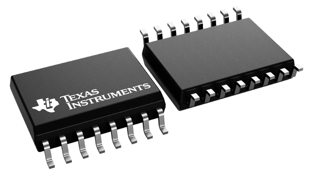
UCC21521
数据:
分类: 微电路 / 半导体集成电路 / 接口电路 / 驱动器
描述: 具有双输入、使能引脚、8V UVLO 且采用 LGA 封装的 5.7kVrms、4A/6A 双通道隔离式栅极驱动器
Number of channels: 2
Isolation rating: Reinforced
Withstand isolation voltage (VISO) (Vrms): 5700
Working isolation voltage (VIOWM) (Vrms): 2121
Transient isolation voltage (VIOTM) (VPK): 8000
Power switch: GaNFET, IGBT, MOSFET, SiCFET
Peak output current (A): 6
Features: Enable, Programmable dead time
Output VCC/VDD (max) (V): 25
Output VCC/VDD (min) (V): 6.5, 9.2, 14.7
Input supply voltage (min) (V): 3
Input supply voltage (max) (V): 18
Propagation delay time (µs): 0.019
Input threshold: CMOS, TTL
Operating temperature range (°C): -40 to 125
Rating: Catalog
Bootstrap supply voltage (max) (V): 2121
Rise time (ns): 6
Fall time (ns): 7
Undervoltage lockout (typ) (V): 5, 8, 12
更多
Number of channels: 2
Isolation rating: Reinforced
Withstand isolation voltage (VISO) (Vrms): 5700
Working isolation voltage (VIOWM) (Vrms): 2121
Transient isolation voltage (VIOTM) (VPK): 8000
Power switch: GaNFET, IGBT, MOSFET, SiCFET
Peak output current (A): 6
Features: Enable, Programmable dead time
Output VCC/VDD (max) (V): 25
Output VCC/VDD (min) (V): 6.5, 9.2, 14.7
Input supply voltage (min) (V): 3
Input supply voltage (max) (V): 18
Propagation delay time (µs): 0.019
Input threshold: CMOS, TTL
Operating temperature range (°C): -40 to 125
Rating: Catalog
Bootstrap supply voltage (max) (V): 2121
Rise time (ns): 6
Fall time (ns): 7
Undervoltage lockout (typ) (V): 5, 8, 12