
Rating: Automotive
Architecture: Gate driver
Control interface: 1xPWM, 3xPWM, 6xPWM, SPI
Gate drive (A): 1
Vs (min) (V): 4.5
Vs ABS (max) (V): 65
Operating temperature range (°C): -40 to 150
TI functional safety category: Functional Safety-Compliant
Rating: Automotive
Architecture: Gate driver
Control interface: 1xPWM, 3xPWM, 6xPWM, SPI
Gate drive (A): 1
Vs (min) (V): 4.5
Vs ABS (max) (V): 65
Operating temperature range (°C): -40 to 150
TI functional safety category: Functional Safety-Compliant
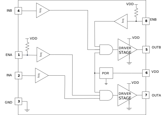
Number of channels: 2
Power switch: IGBT, MOSFET
Peak output current (A): 4
Input supply voltage (min) (V): 4
Input supply voltage (max) (V): 18
Features: Enable pin
Operating temperature range (°C): -40 to 125
Fall time (ns): 7
Input threshold: CMOS, TTL
Channel input logic: Non-Inverting
Input negative voltage (V): -5
Rating: Automotive
Driver configuration: Non-Inverting
Number of channels: 2
Power switch: IGBT, MOSFET
Peak output current (A): 4
Input supply voltage (min) (V): 4
Input supply voltage (max) (V): 18
Features: Enable pin
Operating temperature range (°C): -40 to 125
更多
Fall time (ns): 7
Input threshold: CMOS, TTL
Channel input logic: Non-Inverting
Input negative voltage (V): -5
Rating: Automotive
Driver configuration: Non-Inverting
Number of full bridges: 1
Vs (min) (V): 1.65
Vs ABS (max) (V): 12
Peak output current (A): 4
RDS(ON) (HS + LS) (mΩ): 240
Sleep current (µA): 0.01
Control mode: PWM
Control interface: Hardware (GPIO)
Rating: Catalog
Operating temperature range (°C): -40 to 125
Number of full bridges: 1
Vs (min) (V): 1.65
Vs ABS (max) (V): 12
Peak output current (A): 4
RDS(ON) (HS + LS) (mΩ): 240
Sleep current (µA): 0.01
Control mode: PWM
Control interface: Hardware (GPIO)
Rating: Catalog
Operating temperature range (°C): -40 to 125
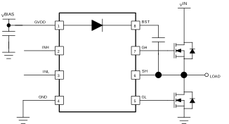
Bootstrap supply voltage (max) (V): 107
Power switch: IGBT, MOSFET
Input supply voltage (min) (V): 9
Input supply voltage (max) (V): 18
Peak output current (A): 0.65
Operating temperature range (°C): -40 to 125
Undervoltage lockout (typ) (V): 8
Rating: Catalog
Fall time (ns): 18
Input threshold: CMOS, TTL
Channel input logic: Noninverting
Switch node voltage (V): -1
Features: Integrated bootstrap diode
Driver configuration: Dual inputs
Bootstrap supply voltage (max) (V): 107
Power switch: IGBT, MOSFET
Input supply voltage (min) (V): 9
Input supply voltage (max) (V): 18
Peak output current (A): 0.65
Operating temperature range (°C): -40 to 125
更多
Undervoltage lockout (typ) (V): 8
Rating: Catalog
Fall time (ns): 18
Input threshold: CMOS, TTL
Channel input logic: Noninverting
Switch node voltage (V): -1
Features: Integrated bootstrap diode
Driver configuration: Dual inputs
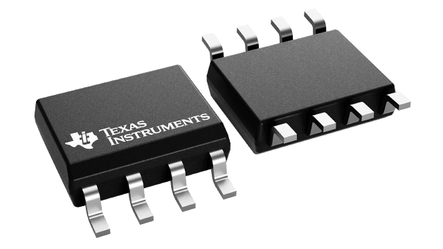
Bootstrap supply voltage (max) (V): 107
Power switch: IGBT, MOSFET
Input supply voltage (min) (V): 9
Input supply voltage (max) (V): 18
Peak output current (A): 0.65
Operating temperature range (°C): -40 to 125
Undervoltage lockout (typ) (V): 8
Rating: Catalog
Fall time (ns): 18
Iq (mA): 0.0333
Input threshold: CMOS, TTL
Channel input logic: Noninverting
Switch node voltage (V): -1
Driver configuration: Dual inputs
Bootstrap supply voltage (max) (V): 107
Power switch: IGBT, MOSFET
Input supply voltage (min) (V): 9
Input supply voltage (max) (V): 18
Peak output current (A): 0.65
Operating temperature range (°C): -40 to 125
更多
Undervoltage lockout (typ) (V): 8
Rating: Catalog
Fall time (ns): 18
Iq (mA): 0.0333
Input threshold: CMOS, TTL
Channel input logic: Noninverting
Switch node voltage (V): -1
Driver configuration: Dual inputs
Bootstrap supply voltage (max) (V): 120
Power switch: MOSFET
Input supply voltage (min) (V): 8
Input supply voltage (max) (V): 17
Peak output current (A): 4
Operating temperature range (°C): -40 to 150
Undervoltage lockout (typ) (V): 8
Rating: Automotive
Propagation delay time (µs): 0.02
Rise time (ns): 7.2
Fall time (ns): 5.5
Iq (mA): 0.001
Input threshold: TTL
Channel input logic: TTL
Switch node voltage (V): -20
Features: Enable, Negative voltage handling
TI functional safety category: Functional Safety-Capable
Driver configuration: Dual, Noninverting, TTL compatible
Bootstrap supply voltage (max) (V): 120
Power switch: MOSFET
更多
Input supply voltage (min) (V): 8
Input supply voltage (max) (V): 17
Peak output current (A): 4
Operating temperature range (°C): -40 to 150
Undervoltage lockout (typ) (V): 8
Rating: Automotive
Propagation delay time (µs): 0.02
Rise time (ns): 7.2
Fall time (ns): 5.5
Iq (mA): 0.001
Input threshold: TTL
Channel input logic: TTL
Switch node voltage (V): -20
Features: Enable, Negative voltage handling
TI functional safety category: Functional Safety-Capable
Driver configuration: Dual, Noninverting, TTL compatible
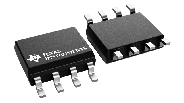
Bootstrap supply voltage (max) (V): 107
Power switch: IGBT, MOSFET
Input supply voltage (min) (V): 9
Input supply voltage (max) (V): 18
Peak output current (A): 0.65
Operating temperature range (°C): -40 to 125
Undervoltage lockout (typ) (V): 8
Rating: Catalog
Fall time (ns): 18
Iq (mA): 0.0333
Input threshold: CMOS, TTL
Channel input logic: Inverting, Noninverting
Switch node voltage (V): -1
Features: Dead time control
Driver configuration: Single input
Bootstrap supply voltage (max) (V): 107
Power switch: IGBT, MOSFET
Input supply voltage (min) (V): 9
Input supply voltage (max) (V): 18
Peak output current (A): 0.65
更多
Operating temperature range (°C): -40 to 125
Undervoltage lockout (typ) (V): 8
Rating: Catalog
Fall time (ns): 18
Iq (mA): 0.0333
Input threshold: CMOS, TTL
Channel input logic: Inverting, Noninverting
Switch node voltage (V): -1
Features: Dead time control
Driver configuration: Single input
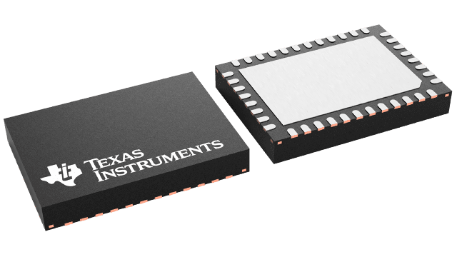
MCF8316C-Q1

数据:
分类: 微电路 / 半导体集成电路 / 接口电路 / 驱动器
描述: 汽车类 40V 最大电压、8A 峰值电流、无传感器场定向控制 (FOC) 三相 BLDC 电机驱动器
Rating: Automotive
Architecture: Integrated FET
Control topology: Field-oriented control (FOC), Sensorless
Control interface: 1xPWM, Analog, Serial
Vs (min) (V): 4.5
Vs ABS (max) (V): 40
Operating temperature range (°C): -40 to 125
Rating: Automotive
Architecture: Integrated FET
Control topology: Field-oriented control (FOC), Sensorless
Control interface: 1xPWM, Analog, Serial
Vs (min) (V): 4.5
Vs ABS (max) (V): 40
Operating temperature range (°C): -40 to 125
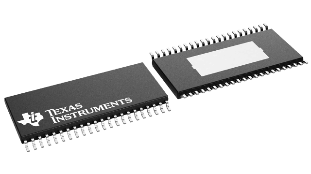
Number of full bridges: 2
Vs (min) (V): 4.5
Vs ABS (max) (V): 70
Peak output current (A): 10
RDS(ON) (HS + LS) (mΩ): 100
Sleep current (µA): 2
Control mode: PH/EN, PWM
Control interface: Hardware (GPIO)
Rating: Catalog
Operating temperature range (°C): -40 to 125
Number of full bridges: 2
Vs (min) (V): 4.5
Vs ABS (max) (V): 70
Peak output current (A): 10
RDS(ON) (HS + LS) (mΩ): 100
Sleep current (µA): 2
Control mode: PH/EN, PWM
Control interface: Hardware (GPIO)
Rating: Catalog
Operating temperature range (°C): -40 to 125
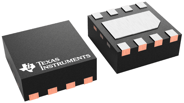
Bootstrap supply voltage (max) (V): 107
Power switch: IGBT, MOSFET
Input supply voltage (min) (V): 5
Input supply voltage (max) (V): 18
Peak output current (A): 0.65
Operating temperature range (°C): -40 to 125
Undervoltage lockout (typ) (V): 5
Rating: Catalog
Propagation delay time (µs): 0.125
Rise time (ns): 28
Fall time (ns): 18
Iq (mA): 0.0333
Input threshold: CMOS, TTL
Channel input logic: Noninverting
Switch node voltage (V): -1
Features: Integrated bootstrap diode
Driver configuration: Dual inputs
Bootstrap supply voltage (max) (V): 107
Power switch: IGBT, MOSFET
Input supply voltage (min) (V): 5
更多
Input supply voltage (max) (V): 18
Peak output current (A): 0.65
Operating temperature range (°C): -40 to 125
Undervoltage lockout (typ) (V): 5
Rating: Catalog
Propagation delay time (µs): 0.125
Rise time (ns): 28
Fall time (ns): 18
Iq (mA): 0.0333
Input threshold: CMOS, TTL
Channel input logic: Noninverting
Switch node voltage (V): -1
Features: Integrated bootstrap diode
Driver configuration: Dual inputs