
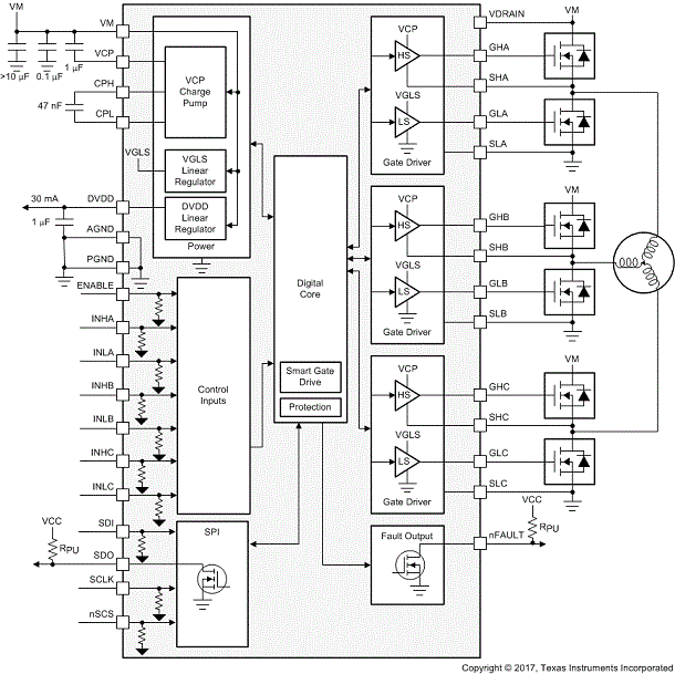

Rating: Catalog
Architecture: Gate driver
Control interface: 1xPWM, 3xPWM, 6xPWM
Gate drive (A): 1
Vs (min) (V): 6
Vs ABS (max) (V): 65
Features: Hardware Management I/F, SPI/I2C, Smart Gate Drive
Operating temperature range (°C): -40 to 125
Rating: Catalog
Architecture: Gate driver
Control interface: 1xPWM, 3xPWM, 6xPWM
Gate drive (A): 1
Vs (min) (V): 6
Vs ABS (max) (V): 65
Features: Hardware Management I/F, SPI/I2C, Smart Gate Drive
Operating temperature range (°C): -40 to 125
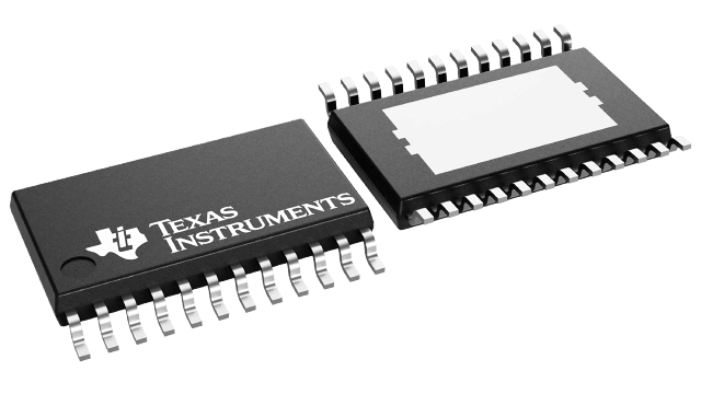
Rating: Automotive
Architecture: Integrated FET
Control topology: Sensorless, Sinusoidal
Control interface: 1xPWM, Analog, Serial
Vs (min) (V): 6.2
Vs ABS (max) (V): 45
Operating temperature range (°C): -40 to 125
Rating: Automotive
Architecture: Integrated FET
Control topology: Sensorless, Sinusoidal
Control interface: 1xPWM, Analog, Serial
Vs (min) (V): 6.2
Vs ABS (max) (V): 45
Operating temperature range (°C): -40 to 125
Rating: Catalog
Architecture: Gate driver
Control interface: 1xPWM, 3xPWM, 6xPWM
Gate drive (A): 1
Vs (min) (V): 6
Vs ABS (max) (V): 65
Operating temperature range (°C): -40 to 125
Rating: Catalog
Architecture: Gate driver
Control interface: 1xPWM, 3xPWM, 6xPWM
Gate drive (A): 1
Vs (min) (V): 6
Vs ABS (max) (V): 65
Operating temperature range (°C): -40 to 125
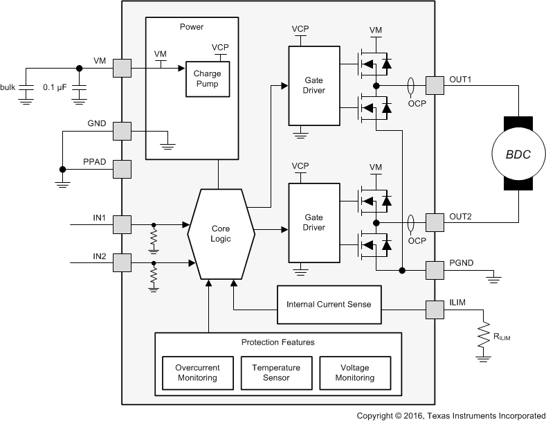
Number of full bridges: 1
Vs (min) (V): 6.5
Vs ABS (max) (V): 50
Peak output current (A): 3.7
RDS(ON) (HS + LS) (mΩ): 565
Sleep current (µA): 13
Control mode: PWM
Control interface: Hardware (GPIO)
Features: Current Regulation, Integrated Current Sensing
Rating: Automotive
TI functional safety category: Functional Safety-Capable
Operating temperature range (°C): -40 to 125
Number of full bridges: 1
Vs (min) (V): 6.5
Vs ABS (max) (V): 50
Peak output current (A): 3.7
RDS(ON) (HS + LS) (mΩ): 565
Sleep current (µA): 13
Control mode: PWM
Control interface: Hardware (GPIO)
更多
Features: Current Regulation, Integrated Current Sensing
Rating: Automotive
TI functional safety category: Functional Safety-Capable
Operating temperature range (°C): -40 to 125
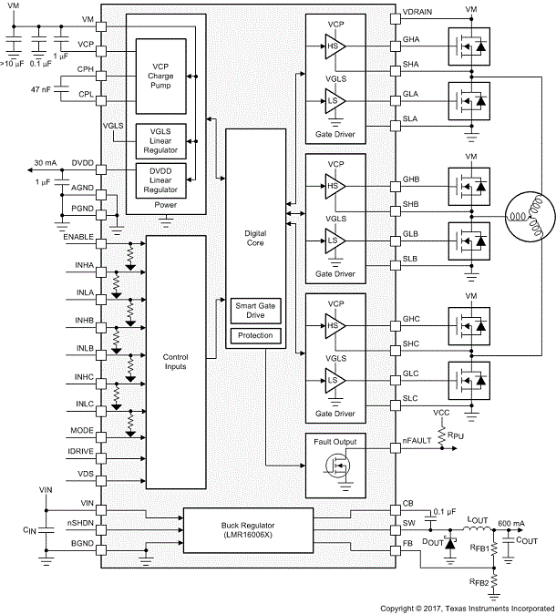
Rating: Catalog
Architecture: Gate driver
Control interface: 1xPWM, 3xPWM, 6xPWM
Gate drive (A): 1
Vs (min) (V): 6
Vs ABS (max) (V): 65
Operating temperature range (°C): -40 to 125
Rating: Catalog
Architecture: Gate driver
Control interface: 1xPWM, 3xPWM, 6xPWM
Gate drive (A): 1
Vs (min) (V): 6
Vs ABS (max) (V): 65
Operating temperature range (°C): -40 to 125
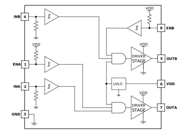
Number of channels: 2
Power switch: GaNFET, IGBT, MOSFET
Peak output current (A): 5
Input supply voltage (min) (V): 4.5
Input supply voltage (max) (V): 18
Features: Enable pin
Operating temperature range (°C): -40 to 140
Rise time (ns): 7
Fall time (ns): 6
Propagation delay time (µs): 0.013
Input threshold: CMOS, TTL
Channel input logic: Dual, Non-Inverting
Input negative voltage (V): -5
Rating: Automotive
Undervoltage lockout (typ) (V): 4
Driver configuration: Dual, Non-Inverting
Number of channels: 2
Power switch: GaNFET, IGBT, MOSFET
Peak output current (A): 5
Input supply voltage (min) (V): 4.5
更多
Input supply voltage (max) (V): 18
Features: Enable pin
Operating temperature range (°C): -40 to 140
Rise time (ns): 7
Fall time (ns): 6
Propagation delay time (µs): 0.013
Input threshold: CMOS, TTL
Channel input logic: Dual, Non-Inverting
Input negative voltage (V): -5
Rating: Automotive
Undervoltage lockout (typ) (V): 4
Driver configuration: Dual, Non-Inverting
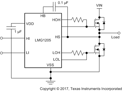
Power switch: GaNFET, MOSFET
Input supply voltage (min) (V): 4.5
Input supply voltage (max) (V): 5.5
Peak output current (A): 5
Operating temperature range (°C): -40 to 125
Undervoltage lockout (typ) (V): 4
Rating: Catalog
Propagation delay time (µs): 0.035
Rise time (ns): 7
Fall time (ns): 3.5
Iq (mA): 0.09
Input threshold: TTL
Channel input logic: TTL
Switch node voltage (V): -5
Driver configuration: Half bridge
Power switch: GaNFET, MOSFET
Input supply voltage (min) (V): 4.5
Input supply voltage (max) (V): 5.5
Peak output current (A): 5
Operating temperature range (°C): -40 to 125
更多
Undervoltage lockout (typ) (V): 4
Rating: Catalog
Propagation delay time (µs): 0.035
Rise time (ns): 7
Fall time (ns): 3.5
Iq (mA): 0.09
Input threshold: TTL
Channel input logic: TTL
Switch node voltage (V): -5
Driver configuration: Half bridge
Number of full bridges: 1/2
Vs (min) (V): 5.5
Vs ABS (max) (V): 47
Sleep current (µA): 14
Control mode: Independent 1/2-Bridge, PWM
Control interface: Hardware (GPIO)
Features: Current Regulation, Current sense Amplifier, Smart Gate Drive
Rating: Automotive
Operating temperature range (°C): -40 to 125
Number of full bridges: 1/2
Vs (min) (V): 5.5
Vs ABS (max) (V): 47
Sleep current (µA): 14
Control mode: Independent 1/2-Bridge, PWM
Control interface: Hardware (GPIO)
Features: Current Regulation, Current sense Amplifier, Smart Gate Drive
Rating: Automotive
Operating temperature range (°C): -40 to 125
Number of full bridges: 1/2
Vs (min) (V): 5.5
Vs ABS (max) (V): 47
Sleep current (µA): 14
Control mode: Independent 1/2-Bridge, PWM
Control interface: Hardware (GPIO), SPI
Features: Current Regulation, Current sense Amplifier, Smart Gate Drive
Rating: Automotive
Operating temperature range (°C): -40 to 125
Number of full bridges: 1/2
Vs (min) (V): 5.5
Vs ABS (max) (V): 47
Sleep current (µA): 14
Control mode: Independent 1/2-Bridge, PWM
Control interface: Hardware (GPIO), SPI
Features: Current Regulation, Current sense Amplifier, Smart Gate Drive
Rating: Automotive
Operating temperature range (°C): -40 to 125
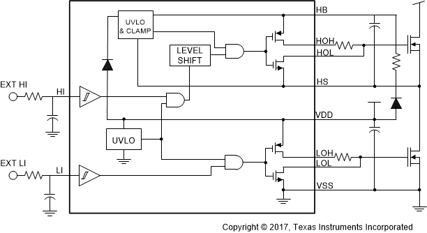
Bootstrap supply voltage (max) (V): 100
Power switch: GaNFET, MOSFET
Input supply voltage (min) (V): 4.5
Input supply voltage (max) (V): 5.5
Peak output current (A): 5
Operating temperature range (°C): -40 to 125
Undervoltage lockout (typ) (V): 4
Rating: Automotive
Propagation delay time (µs): 0.03
Rise time (ns): 7
Fall time (ns): 3.5
Iq (mA): 0.15
Input threshold: TTL
Channel input logic: TTL
Switch node voltage (V): -5
Driver configuration: Half bridge
Bootstrap supply voltage (max) (V): 100
Power switch: GaNFET, MOSFET
Input supply voltage (min) (V): 4.5
Input supply voltage (max) (V): 5.5
更多
Peak output current (A): 5
Operating temperature range (°C): -40 to 125
Undervoltage lockout (typ) (V): 4
Rating: Automotive
Propagation delay time (µs): 0.03
Rise time (ns): 7
Fall time (ns): 3.5
Iq (mA): 0.15
Input threshold: TTL
Channel input logic: TTL
Switch node voltage (V): -5
Driver configuration: Half bridge